

How To Access The Contents Of Registers In Arm Keil Software
This is the Series of tutorials on STM32 Microcontroller. The aim of this series is to provide easy and practical examples that anyone tin sympathize. Basically, you tin write GPIO codes in multiple ways (Using HAL, GPIO driver). Using that HAL you lot tin can finish your chore in ane line of code. But I would suggest you lot, larn to program using the bare-metal code (without any HAL or commuter) initially. This is the STM32 GPIO Tutorial without HAL.
You can also read, Getting started with STM32 RTOS, PIC16F877A GPIO tutorial, GPIO Linux device commuter, and STM32 GPIO RTOS tutorial.
Prerequisites
Before starting this STM32 GPIO Tutorial, Please get through the below tutorials.
- Create a New Projection for STM32 in Keil
STM32 GPIO Tutorial
Introduction
GPIO stands for "General Purpose Input/Output." We are using STM32F401VE for our examples. STM32F401VE has v ports mentioned beneath.
- PORT A
- PORT B
- PORT C
- PORT D
- PORT Due east
Each port has 16 GPIO pins.
GPIO main features
- Up to xvi I/Os under control
- Output states: push-pull or open up-drain + pull-up/down
- Output data from output information annals (
GPIOx_ODR) or peripheral (alternate function output) - Speed selection for each I/O
- Input states: floating, pull-up/downwards, analog
- Input information to input data register (
GPIOx_IDR) or peripheral (alternating function input) - Flake set and reset annals (
GPIOx_BSRR) for bitwise write access toGPIOx_ODR - Locking machinery (
GPIOx_LCKR) provided to freeze the I/O configuration - Analog part
- Alternate function input/output pick registers (at most 16 AFs per I/O)
- Fast toggle capable of irresolute every 2 clock cycles
- Highly flexible pin multiplexing allows the employ of I/O pins every bit GPIOs or as one of several peripheral functions
STM32 GPIO Tutorial – Registers used in STM32 GPIO
At that place are a couple of registers used in GPIO. I have classified these register into 4 types based on their operation.
- Control Registers
- Information Registers
- Locking Registers
- Alternate Function Registers
Control Registers
Before looking into the control register, we will see the Clock Register ( RCC_AHB1ENR ) which will enable the AHB clock to the GPIO ports.
RCC_AHB1ENR
This is called as RCC AHB1 peripheral clock enable register. The register is given below.
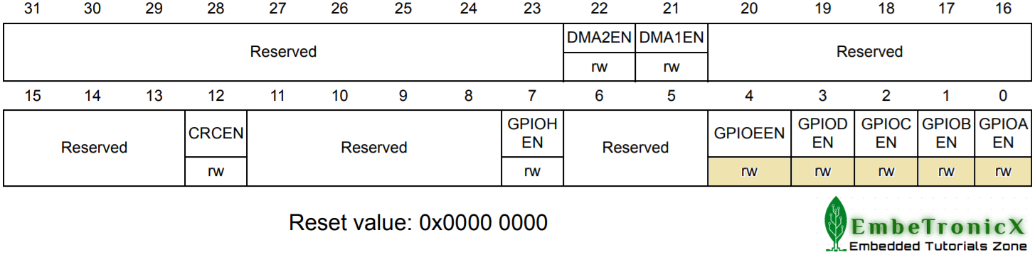
Bit [0] – GPIOAEN: IO port A clock enable
- 0 – IO port A clock disabled
- 1 – IO port A clock enabled
Scrap [1] – GPIOBEN: IO port B clock enable
- 0 – IO port B clock disabled
- one – IO port B clock enabled
Bit [2] – GPIOBEN: IO port C clock enable
- 0 – IO port C clock disabled
- 1 – IO port C clock enabled
Bit [3] – GPIOBEN: IO port D clock enable
- 0 – IO port D clock disabled
- 1 – IO port D clock enabled
Bit [4] – GPIOBEN: IO port E clock enable
- 0 – IO port E clock disabled
- i – IO port East clock enabled
We don't demand the remainder of the bits as nosotros are merely working on GPIO.
Example
//These are a couple of means of enabling AHB clock for Port A SET_BIT(RCC->AHB1ENR, RCC_AHB1ENR_GPIOAEN); RCC->AHB1ENR |= (1UL << 0U);
The below control registers are used to configure the GPIOs.
- GPIO Port manner register (
GPIOx_MODER) - GPIO Port output type register (
GPIOx_OTYPER) - GPIO Port output speed register (
GPIOx_OSPEEDR) - GPIO Port Pullup/Pulldown register (
GPIOx_PUPDR)
GPIOx_MODER
This GPIO port mode annals is used to select the I/O management. Please notice the below image of the GPIOx_MODER register.
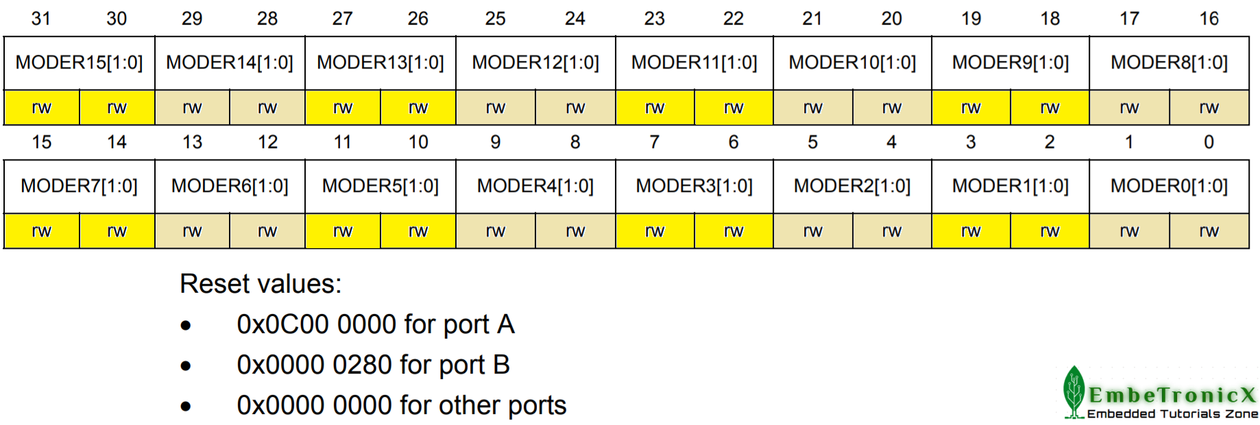 Hither 2-bits are combined for one particular GPIO pin.
Bits [31:0] – MODERy : Direction selection for port Ten and bit Y, (y = 0 … xv)
MODERy Direction Selection:
00: Input (reset state)
01: General purpose output mode
10: Alternate Function way
11: Analog mode
In this tutorial, we are using only the I/O operation. And so, we will apply either Input way or output mode.
Example
//makes Port A0 as output GPIOA->MODER = 0x00000001; //makes Port A5 as output GPIOA->MODER = 0x00000400; //makes Port A every bit output GPIOA->MODER = 0x55555555; //makes Port A every bit input GPIOA->MODER = 0x00000000;
GPIOx_OTYPER
This is the GPIO output blazon annals which is used to select the output type (Push-Pull or Open Bleed). Kickoff, nosotros need to know what is push button-pull and open drain.
Open-bleed output type
I think well-nigh of them are aware of this. If you have worked on I2C you must have heard this. But still, I will put my words. In open-drain mode, inside the microcontroller i switch (transistor/MOSFET) is continued to the GPIO pivot and the footing. So If you write high to the GPIO pin using software, it volition be continued to the ground through the switch. Which ways the original output is low. If you write low to the GPIO pin, it will be left floating since the switch will be turned off. That's why nosotros are using a pullup resistor for the open-drain pins.
Button-Pull output type
Whereas in button-pull mode, two switches (transistor/MOSFET) will be there inside of the microcontroller. I switch is continued to Vcc/Vdd and another switch is connected to the ground. And then when you write Loftier to the GPIO pivot, the switch will be connected to the Vcc/Vdd. The resulting output will be high (1). And if you write low to the GPIO, then the switch volition be continued to the ground. The resulting output will be low (0).
Got some thought well-nigh both output modes? Okay, let's get to the annals now. Delight find the beneath image of the GPIOx_OTYPER annals.
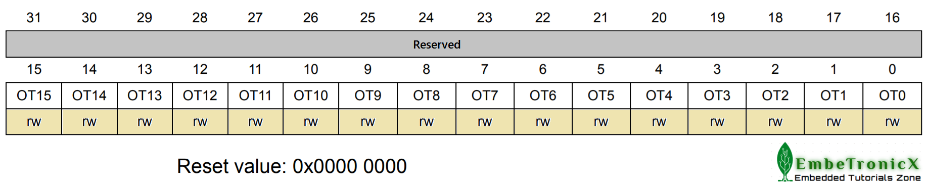
Here,
Bits [15:0] – OTy : Port output type, (y = 0 … 15)
- 0 – Output Push button-Pull (reset state)
- i – Output open-bleed
Bits [31:16] – Reserved (Must be kept at reset value).
GPIOx_OSPEEDR
This GPIO Output speed register is used to fix the speed of the GPIO pin. Please find the beneath image of the GPIOx_OSPEEDR register.
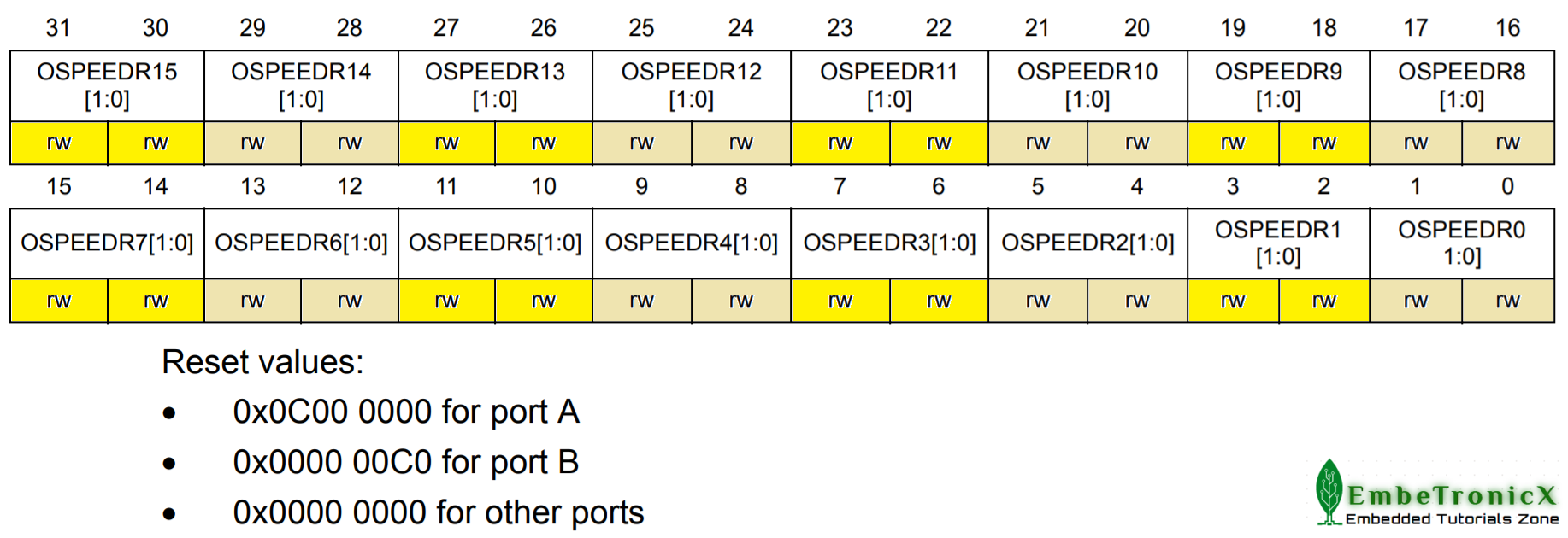 Here 2-bits are combined for one particular GPIO pivot.
Bits [31:0] – OSPEEDRy : Speed selection for port 10 and bit Y, (y = 0 … 15)
OSPEEDRy Selection:
00: Depression Speed
01: Medium speed
10: High speed
eleven: Very high speed
GPIOx_PUPDR
This is the GPIO port pullup/pulldown register which is used to configure the GPIO pin into Pullup or pulldown style. Please detect the beneath image of the GPIOx_PUPDR annals.
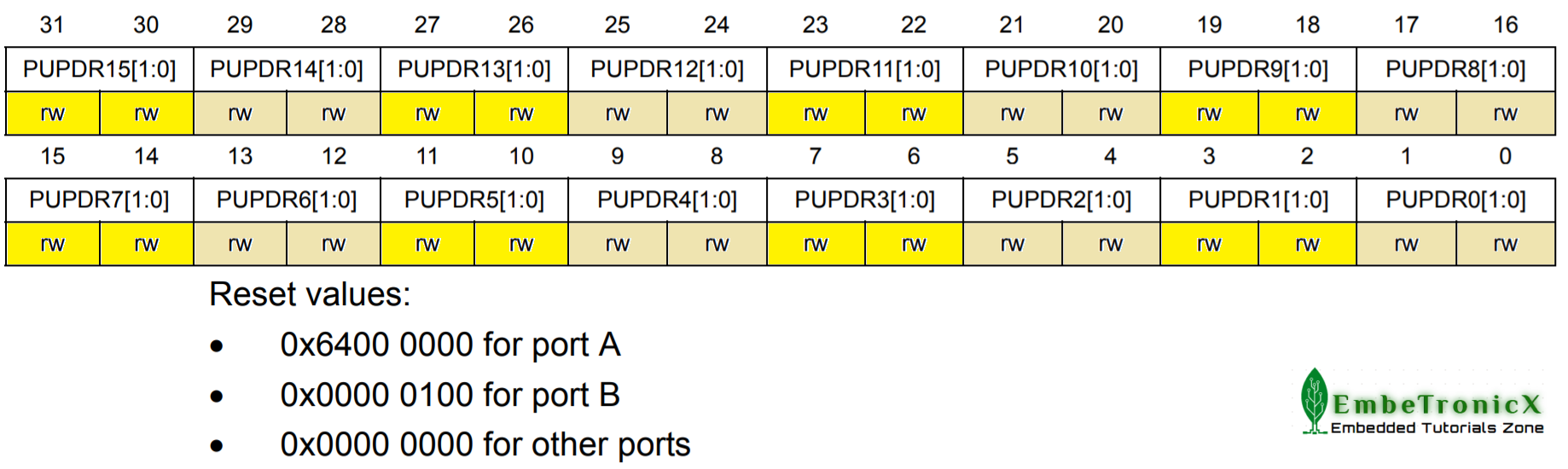 Here 2-bits are combined for one detail GPIO pin.
$.25 [31:0] – PUPDRy : pullup/pulldown option for port 10 and fleck Y, (y = 0 … 15)
PUPDRy Selection:
00: No pullup or pulldown
01: Pullup
10: Pulldown
11: Reserved
Case
//Enable Pullup on PA0 GPIOA->PUPDR = 0x00000001; //Enable Pullup on PA GPIOA->PUPDR = 0x55555555;
Information Registers
These data registers are used to make the store the data to be output/input. The beneath registers are used for output/input.
- Input data register (
GPIOx_IDR) - Output data register (
GPIOx_ODR) - Scrap Set/Reset register (
GPIOx_BSRR)
where, x = A, B, C, D, and E.
GPIOx_IDR
This is the Input Data Register. When yous configure the GPIO ports every bit input using GPIOx_MODER register, this annals is used to become the value from the GPIO pin. This register is a read-only register. And so you lot cannot write into it. Delight find the below image of the GPIOx_IDR register.
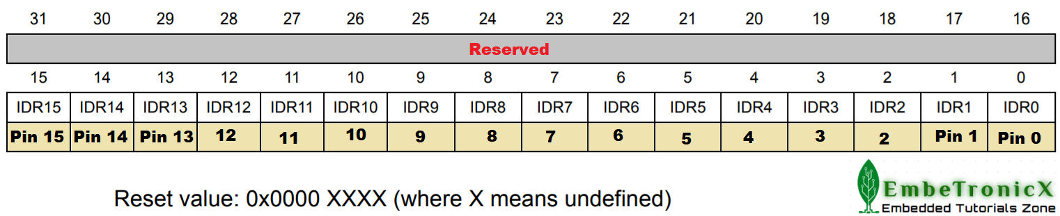 Here,
Here,
Bits [15:0] – IDRy : Port Input Information, (y = 0 … 15)
This will be containing the corresponding value of the corresponding I/O port. And It can exist accessed in 32-bit give-and-take way only. Which means you cannot read a single bit. You have to read the whole register.
Bits [31:16] – Reserved (Must exist kept at reset value).
Example
Let's assume that I have configured PORT B as input, using the GPIOB_MODER register and other control registers. Now we can read the GPIO pins like below.
//Reading PB0 chip if( ( GPIOB->IDR & 0x01) == 0 ) { //PORT B'south 0th fleck is 0 } else { //PORT B's 0th bit is 1 } //Reading total PB uint32_t value = GPIOB->IDR; //Reading PB15 bool value = (( GPIOB->IDR >> xv ) & 0x1); GPIOx_ODR
This is the Output Data Register. When you lot take configured GPIO Port as output using GPIOx_MODER register, this register is used to ready the value to the GPIO pin. We can read and write to the annals. Please detect the below image of the GPIOx_ODR annals.
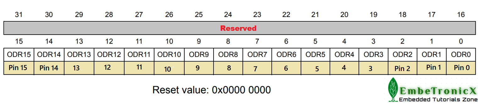
Bits [xv:0] – ODRy : Port Output Data, (y = 0 … fifteen)
We tin can write to the respective value of the corresponding I/O port.
$.25 [31:16] – Reserved (Must exist kept at reset value).
Note: When yous read the output data register, information technology will give you the terminal written value.
Case
Allow'due south assume that I have configured PORT B every bit output, using the GPIOB_MODER register and other control registers. Now we tin can write the GPIO pins like below.
//Write ane to the full Port B GPIOB->ODR = 0x0000FFFF; //Write 0 to the full Port B GPIOB->ODR = 0x00000000;
Yous take to exist conscientious when you are writing the GPIO port using this GPIOx_ODR . Because you may disturb the other Pins (bits) of the register which you don't want to. So what if I want to write a unmarried fleck without agonizing others? There is a way to do that. Just keep reading.
GPIOx_BSRR
This is GPIO Bit Prepare/Reset Register. When you want to set or reset the particular bit or pivot, you lot can use this register. This is a write-only annals. This register volition do the diminutive set/reset. So we don't worry about the interrupts that causing problems during gear up/reset. And in this register, the lower sixteen-bits are used to set whatsoever of the 16 pins and the higher 16-bits to clear/reset any of the 16 pins of a item IO port. Delight discover the below image of the GPIOx_BSRR annals.
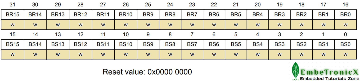
Bits [15:0] – BSy : Port Set Bit, (y = 0 … fifteen)
These $.25 are write-only and accessed in word, one-half-word, or byte mode. If you read this register you will get 0x00000000. If you write i to whatever flake [0 to 15], it will set the corresponding scrap in GPIOx_ODR register [0 to 15]. If you lot write 0 to whatsoever bit [0 to 15], no activity will exist performed to the corresponding chip in GPIOx_ODR annals [0 to 15].
Bits [31:sixteen] – BRy : Port Reset Fleck, (y = 0 … fifteen)
These $.25 are write-but and accessed in word, half-word, or byte mode. If you read this register you will get 0x00000000. If you lot write 1 to any fleck [16 to 31], information technology will set the respective bit in GPIOx_ODR annals [0 to 15]. If you write 0 to whatsoever bit [0 to 15], no action volition be performed to the corresponding chip in GPIOx_ODR register [0 to xv].
If you ready both BSx and BRx , BSx has the priority. So BRx will exist ignored. Where, ten = 0…15.
Example
Let'south assume that I accept configured PORT B as output, using the GPIOB_MODER register and other command registers. Now we can write the GPIO pins like below.
//set all the bits of Port B GPIOB->BSRR = 0x0000FFFF; //Clear all the bits of Port B GPIOB->BSRR = 0xFFFF0000; //Set the 5th bit of Port B GPIOB->BSRR = (1U << v); //Clear the 5th bit of Port B GPIOB->BSRR = (1U << 21);
Locking Registers
This register is used to lock the configuration of the port bits. The below register is used to practise that.
- GPIO Lock register (
GPIOx_LCKR)
GPIOx_LCKR
Using this register, you can freeze the GPIO configurations. In one case you practise the proper lock key write sequence, it volition lock the GPIOx_MODER , GPIOx_OTYPER , GPIOx_OSPEEDR , GPIOx_PUPDR , GPIOx_AFRL , and GPIOx_AFRH registers. Earlier we see how to do that, let's come across that register. Please find the below paradigm of the GPIOx_LCKR register.
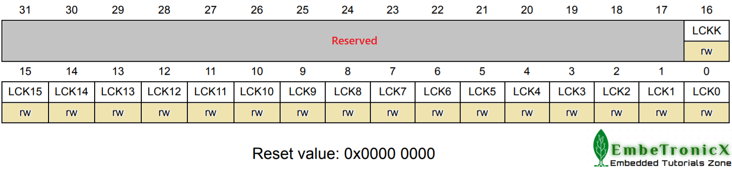 This can be accessed 32-bit word simply and you tin perform both read and write.
Bits [15:0] – LCKy : Port Gear up Bit, (y = 0 … fifteen)
- 0 – Port configuration is not locked
- i – Port configuration is locked
These bits can be written when the LCKK (16th bit) is 0.
$.25 [16] – LCKK : Lock Key
- 0 – Port configuration lock key is not active
- one – Port configuration lock key is not active
This bit can be read at any time. Simply if we want to modify the bit, nosotros have to follow the Lock key write sequence. Once you take locked the GPIO, and so it will exist locked until an MCU reset or a peripheral reset occurs.
$.25 [31:17] – Reserved (Must be kept at reset value).
Lock cardinal write sequence
As per the datasheet, below is the lock cardinal write sequence.
WR LCKR [ sixteen ] = '1' + LCKR [ fifteen : 0 ]
WR LCKR [ xvi ] = '0' + LCKR [ 15 : 0 ]
WR LCKR [ sixteen ] = '1' + LCKR [ 15 : 0 ]
RD LCKR
RD LCKR [ 16 ] = 'one' ( this read operation is optional just it confirms that the lock is active )
Note:During the Lock central write sequence, the value of LCK[xv:0] should not alter. And in some other STM32, this GPIOx_LCKR is not available for all the GPIO ports. So you should check with the datasheet before doing this. But in the STM32F401VE, GPIOx_LCKR register is available for all the GPIO ports.
Whatever error in the lock key write sequence aborts the lock. Once you accept done the lock key write sequence properly on any chip of the port, any read access on the LCKK bit will return '1' until the side by side CPU reset.
If y'all get confused, delight go through the below example.
/* ** The below total lawmaking snippet, locks the GPIO configuration of Port B.5 (PB5) */ #ascertain GPIO_PIN_POS (5U) //I want to lock PB5. So setting 5th bit #ascertain LCKK_BIT_POS (16U) //Position of LCKK fleck volatile uint32_t lock_gpio = 0; /* Lock central write sequence */ /* WR LCKR[sixteen] = 'i' + LCKR[5] = '1' */ lock_gpio = (( 1UL << LCKK_BIT_POS) | ( 1UL << GPIO_PIN_POS )); GPIOB->LCKR = lock_gpio; /* WR LCKR[xvi] = '0' + LCKR[5] should not change*/ GPIOB->LCKR = ( 1UL << GPIO_PIN_POS ); /* WR LCKR[sixteen] = '1' + LCKR[5] should not change*/ GPIOB->LCKR = lock_gpio; /* RD LCKR */ lock_gpio = GPIOB->LCKR; if((GPIOB->LCKR & ( 1UL << LCKK_BIT_POS)) != 0) { //PB5 configuration has been locked } else { //PB5 configuration has not been locked } Alternate Function Registers
Each GPIO pin has around sixteen alternative functions similar SPI, I2C, UART, etc. So we can tell the STM32 to apply our required functions.
The below-mentioned 2 registers are used to select the one function out of sixteen alternative function inputs/outputs available for each I/O.
- Alternate Function Low annals (
GPIOx_AFRL) - Alternate Office High register (
GPIOx_AFRH)
GPIOx_AFRL
This 32-chip register is grouped by 4bits. Then This GPIOx_AFRL register is used to select the alternate functions of Pivot 0 to Pin vii. Please find the below image of the GPIOx_AFRL register.
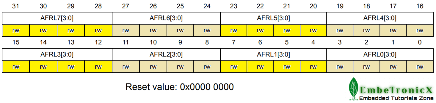 Bits [31:0] – AFRLy : Alternate role selection for port Ten and chip Y, (y = 0 … 7)
AFRLy Selection:
0000: AF0 (Alternate Function 0)
0001: AF1 (Alternating Function i)
0010: AF2 (Alternate Office 2)
0011: AF3 (Alternate Function 3)
0100: AF4 (Alternating Function four)
0101: AF5 (Alternate Function five)
0110: AF6 (Alternate Function half dozen)
0111: AF7 (Alternate Role 7)
m: AF8 (Alternating Function eight)
1001: AF9 (Alternate Role ix)
1010: AF10 (Alternate Role 10)
1011: AF11 (Alternate Part 11)
1100: AF12 (Alternating Function 12)
1101: AF13 (Alternate Role 13)
1110: AF14 (Alternate Function xiv)
1111: AF15 (Alternating Office 15)
GPIOx_AFRH
This 32-scrap annals is grouped by 4bits. So This GPIOx_AFRH annals is used to select the alternating functions of Pivot 8 to Pin 15. Please find the below image of the GPIOx_AFRH register.
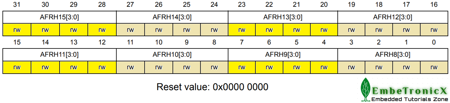
$.25 [31:0] – AFRHy : Alternating function selection for port Ten and chip Y, (y = 0 … 7)
AFRHy Selection:
0000: AF0 (Alternate Function 0)
0001: AF1 (Alternating Role 1)
0010: AF2 (Alternate Role 2)
0011: AF3 (Alternating Function 3)
0100: AF4 (Alternate Part 4)
0101: AF5 (Alternating Function 5)
0110: AF6 (Alternate Function vi)
0111: AF7 (Alternate Function vii)
thou: AF8 (Alternate Function 8)
1001: AF9 (Alternating Function ix)
1010: AF10 (Alternating Part 10)
1011: AF11 (Alternating Function 11)
1100: AF12 (Alternating Office 12)
1101: AF13 (Alternate Function thirteen)
1110: AF14 (Alternate Office 14)
1111: AF15 (Alternating Part 15)
As of now, nosotros are using these pins as a GPIO and we are not selecting other functions than Input/Output. Then in our time to come post, we will hash out these GPIOx_AFRL and GPIOx_AFRH .
I retrieve nosotros have covered almost all the registers. Now we will just put them all together and make our hands muddy by playing with the LEDs. Let's dive into the programming office.
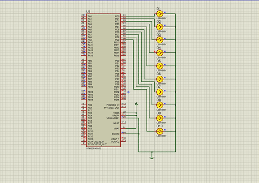
STM32 GPIO Tutorial – LED Interfacing with STM32
In the below instance, I have enabled all the Ports (A, B, C, D, and E) as an output. and toggling them with some delay. You can likewise notice the complete project on GitHub.
Code
/***************************************************************************//** * \file main.c * * \details Setting all the Ports (A, B, C, D, and E) as output * and toggling them with some random delay - STM32 GPIO Tutorial * * \author EmbeTronicX * * \This code is verified with proteus simulation * *******************************************************************************/ #include "stm32f4xx.h" #define DELAY_COUNT ( 30000 ) //delay count /***************************************************************************//** \details Providing Delay by running empty for loop \return void \retval none *******************************************************************************/ static void delay( void ) { uint32_t i = 0; for( i=0; i<=DELAY_COUNT; i++ ); } /***************************************************************************//** \details The main function. It should not return. \return void \retval none *******************************************************************************/ int main(void){ //Enable the AHB clock all GPIO ports SET_BIT(RCC->AHB1ENR, RCC_AHB1ENR_GPIOAEN); SET_BIT(RCC->AHB1ENR, RCC_AHB1ENR_GPIOBEN); SET_BIT(RCC->AHB1ENR, RCC_AHB1ENR_GPIOCEN); SET_BIT(RCC->AHB1ENR, RCC_AHB1ENR_GPIODEN); SET_BIT(RCC->AHB1ENR, RCC_AHB1ENR_GPIOEEN); //set all Port A to Port E as output GPIOA->MODER = 0x55555555; GPIOB->MODER = 0x55555555; GPIOC->MODER = 0x55555555; GPIOD->MODER = 0x55555555; GPIOE->MODER = 0x55555555; //Endless loop while(1){ //Plough ON the LED of all the ports GPIOA->BSRR = 0x0000FFFF; GPIOB->BSRR = 0x0000FFFF; GPIOC->BSRR = 0x0000FFFF; GPIOD->BSRR = 0x0000FFFF; GPIOE->BSRR = 0x0000FFFF; delay(); //Turn OFF the LED of all the ports GPIOA->BSRR = 0xFFFF0000; GPIOB->BSRR = 0xFFFF0000; GPIOC->BSRR = 0xFFFF0000; GPIOD->BSRR = 0xFFFF0000; GPIOE->BSRR = 0xFFFF0000; delay(); } } Output
Please notice the output of the example below.
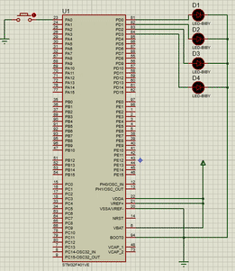
STM32 GPIO Tutorial – Switch/Push button interfacing with STM32
I take connected the button to the PA0 (Port A.0) and LEDs to the PD0 to PD3. Y'all can likewise notice the project on GitHub.
Code
/***************************************************************************//** * \file primary.c * * \details Setting PORT D0 to D3 as output and PORT A0 as input. * When we press the Port A0, we will plough on the PD0-PD3. - STM32 GPIO Tutorial * * \author EmbeTronicX * * \This code is verified with proteus simulation * *******************************************************************************/ #include "stm32f4xx.h" /***************************************************************************//** \details The main function. It should not return. \render void \retval none *******************************************************************************/ int main(void){ //Enable the AHB clock all GPIO PORT A and PORT D SET_BIT(RCC->AHB1ENR, RCC_AHB1ENR_GPIOAEN); SET_BIT(RCC->AHB1ENR, RCC_AHB1ENR_GPIODEN); //set Port A as input GPIOA->MODER = 0x00000000; //Enable Pullup on PA0 GPIOA->PUPDR = 0x00000001; //set PORTD0 to PORTD3 as output GPIOD->MODER = 0x00000055; //Plough OFF the LEDs of PORTD GPIOD->BSRR = 0xFFFF0000; //Endless loop while(1){ //Button is connected to PA0. Then we need to cheque bit 0 of IDR register. if( ( GPIOA->IDR & 0x01) == 0 ) { //Turn ON the LEDs GPIOD->BSRR = 0x0000000F; } else { //Turn OFF the LEDs GPIOD->BSRR = 0x000F0000; } } } Output
Please find the output of the example below.
Note: The code is tested with the Proteus simulation. Not with the real hardware. If y'all take figured out whatsoever problems and issues with code while testing with the hardware, Please inform united states and provide the states as the workaround. So that, We will update here also. This will assistance others to learn.
If you want to use RTOS in STM32, you lot tin can refer to the STM32 GPIO with the RTOS tutorial.
You lot tin also read the below tutorials.
| Linux Device Driver Tutorials | C Programming Tutorials |
| FreeRTOS Tutorials | NuttX RTOS Tutorials |
| RTX RTOS Tutorials | Interrupts Nuts |
| I2C Protocol – Part one (Basics) | I2C Protocol – Part 2 (Avant-garde Topics) |
| STM32 Tutorials | LPC2148 (ARM7) Tutorials |
| PIC16F877A Tutorials | 8051 Tutorials |
| Unit of measurement Testing in C Tutorials | ESP32-IDF Tutorials |
| Raspberry Pi Tutorials | Embedded Interview Topics |
| Reset Sequence in ARM Cortex-M4 | BLE Basics |
| VIC and NVIC in ARM | SPI – Serial Peripheral Interface Protocol |
| Bootloader Tutorials | Raspberry PI Pico Tutorials |
| Zephyr RTOS Tutorials - STM32 | Zephyr RTOS Tutorials - ESP32 |
![]()
Embedded Software | Firmware | Linux Devic Deriver | RTOS

How To Access The Contents Of Registers In Arm Keil Software,
Source: https://embetronicx.com/tutorials/microcontrollers/stm32/stm32-gpio-tutorial/
Posted by: joneswaseltory1969.blogspot.com
0 Response to "How To Access The Contents Of Registers In Arm Keil Software"
Post a Comment